General Description
This document explains the function and use of the RTQ2823A evaluation board (EVB), the RTQ2823A is a high-performance, synchronous step-down converter that can deliver up to 8A output currentvwith an input supply voltage range of 4.5V to 17V. The device integrates low RDS(ON) power MOSFETs, accurate 0.6V reference and an integrated diode for bootstrap circuit to offer a very compact solution. This document explains the function and use of the RTQ2823A evaluation board (EVB), and provides information to enable operation, modification of the evaluation board and circuit to meet individual requirements.
Performance Specification Summary
Summary of the RTQ2823AGQVF Evaluation Board performance specificiaiton is provided in Table 1. The ambient temperature is 25°C.
Table 1. RTQ2823AGQVF Evaluation Board Performance Specification Summary
|
Specification
|
Test Conditions
|
Min
|
Typ
|
Max
|
Unit
|
|
Default Input Voltage
|
Default = 12V
|
4.5
|
12
|
17
|
V
|
|
Output Voltage
|
Default = 1.2V
|
0.6
|
--
|
5.5
|
V
|
|
Maximum Output Current
|
|
--
|
--
|
8
|
A
|
|
Operation Frequency
|
Default = 800kHz
|
400
|
800
|
1200
|
kHz
|
|
Soft-Start Time
|
CSS = 47nF
|
--
|
4.7
|
--
|
ms
|
Power-up Procedure
Suggestion Required Equipments
- DC Power Supply (Chroma, 62006P-100-25)
- Electronic load capable of 30A
- Four Channels Digital Real-Time Oscilloscope
- Display Multi-meter (34405A)
Power-up & Measurement Procedure
1. Apply a 12V nominal input power supply (4.5V < VIN < 17V) to the VIN and GND terminals.
2. Set the jumper at JP1 to connect terminals H and EN, connecting EN to VIN through resistor R18 (100kΩ). The Enable pin can connected to VIN directly as well to enable operation.
3. Set the jumper at JP2 to connect terminals H and PGOOD, Connenting VCC to H through resistor RPGOOD (100kΩ).
4. Verify the output voltage (approximately 1.2V) between VOUT and GND.
5. Connect an external load up to 8A to the VOUT and GND terminals and verify the output voltage and current.
Detailed Description of Hardware
Headers Description and Placement
Carefully inspect all the components used in the EVB according to the following Bill of Materials table, and then make sure all the components are undamaged and correctly installed. If there is any missing or damaged component, which may occur during transportation, please contact our distributors or e-mail us at evb_service@richtek.com.
Test Points
The EVB is provided with the test points and pin names listed in the table below.
|
Test point/
Pin Name
|
Function
|
|
EN
|
Enable Control Input
|
|
MODE
|
Current limit, switching frequency, and light load operation mode selection pin.
|
|
BOOT
|
Bootstrap
|
|
SW
|
Switch node
|
|
PGND
|
Power ground
|
|
VIN
|
Input voltage
|
|
VCC
|
4.7V internal LDO output
|
|
AGND
|
Analog GND
|
|
PGOOD
|
Power good indicator output
|
|
SS
|
Soft-start time control pin
|
Bill of Materials
|
Reference
|
Qty
|
Part Number
|
Description
|
Package
|
Manufacturer
|
|
U4
|
1
|
RTQ2823AGQVF
|
Step-Down
DC-DC Converter
|
VQFN-18L
3.5x3.5 (FC)
|
RICHTEK
|
|
C1, C2,
C7, C15
|
4
|
0603B104K500CT
|
0.1μF, 50V, X7R
|
0603
|
WALSIN
|
|
C3, C4,
C5, C6
|
4
|
GRM21BR61E226ME44L
|
22μF, 25V, X5R
|
0805
|
MURATA
|
|
C11, C12, C13, C14
|
4
|
GRM32ER61C476KE15L
|
47μF, 16V, ±20%, X5R,
|
1210
|
MURATA
|
|
C16
|
1
|
0603N101J500CT
|
100pF, 50V, NPO
|
0603
|
MURATA
|
|
C17
|
1
|
GRM188R71C473KA01
|
0.047μF, 16V, ±10%, X7R
|
0603
|
MURATA
|
|
C19
|
1
|
GRM188R61E475KE11D
|
4.7μF, 10V, ±20%, X5R
|
0603
|
MURATA
|
|
L1
|
1
|
744311068
|
0.68µH, RDC = 3.1mΩ
|
7.0x7.0x4.0
|
WURTH ELEKTRONIK
|
|
R1, R14
R16
|
3
|
WR06X000 PTL
|
RES, 0, 1%, 0.1W
|
0603
|
WALSIN
|
|
R13, R17
|
2
|
WR06X1002FTL
|
RES, 10k, 1%, 0.1W
|
0603
|
WALSIN
|
|
R18, R19
RPGOOD1
|
3
|
WR06X1003FTL
|
RES, 100k, 1%, 0.1W
|
0603
|
WALSIN
|
|
RMODE1
|
1
|
WR06X1203FTL
|
RES, 120k, 1%, 0.1W
|
0603
|
WALSIN
|
|
RMODE2
|
1
|
WR06X2002FTL
|
RES, 20k, 1%, 0.1W
|
0603
|
WALSIN
|
Typical Applications
EVB Schematic Diagram
RTQ2823A demo board: VIN = 12V, VOUT 1.2V / 8A
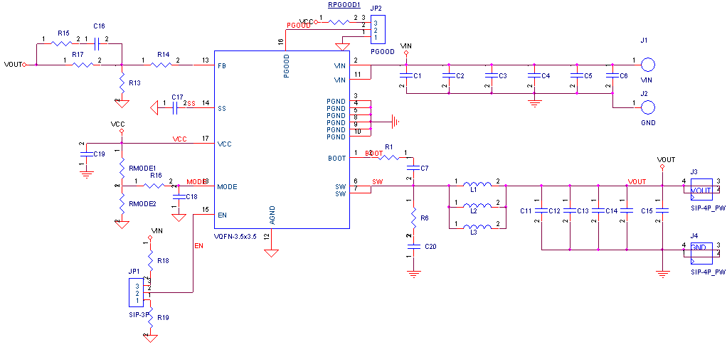
Note :
1. The capacitance values of the input and output capacitors will influence the input and output voltage ripple.
2. MLCC capacitors have degrading capacitance at DC bias voltage, and especially smaller size MLCC capacitors will have much lower capacitance than specified.
3. Set default soft start time 5ms by connecting C17 to 47nF.
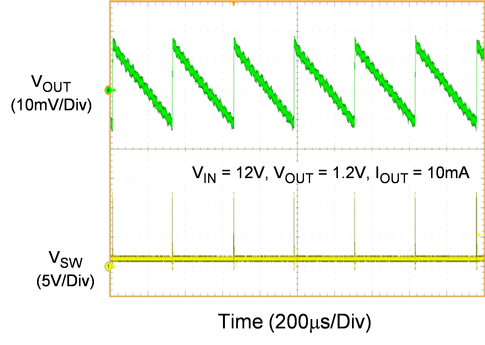
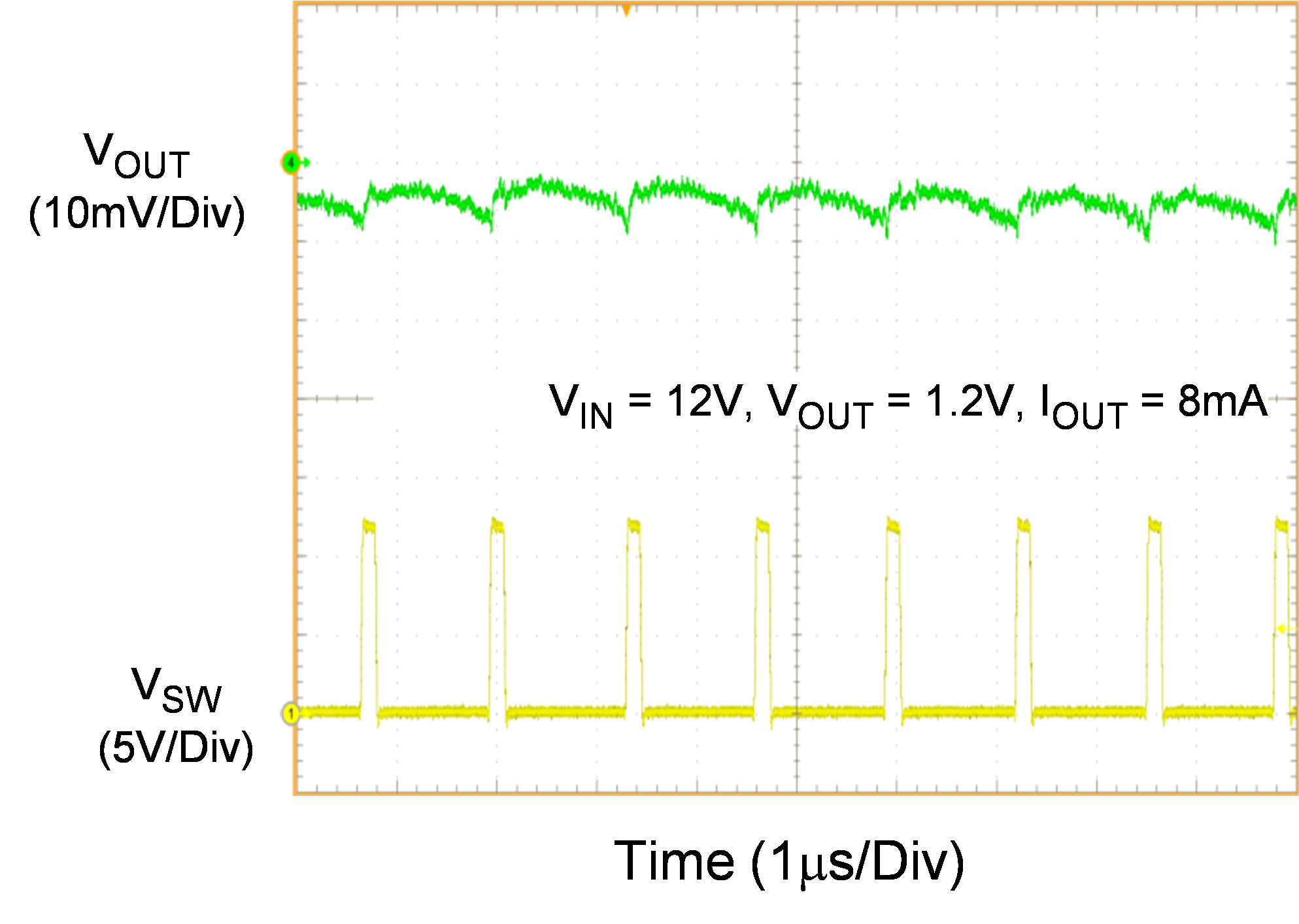
Measurement Results
|
Output Ripple Measurement
|
Output Ripple Measurement
|
|
|
|
|
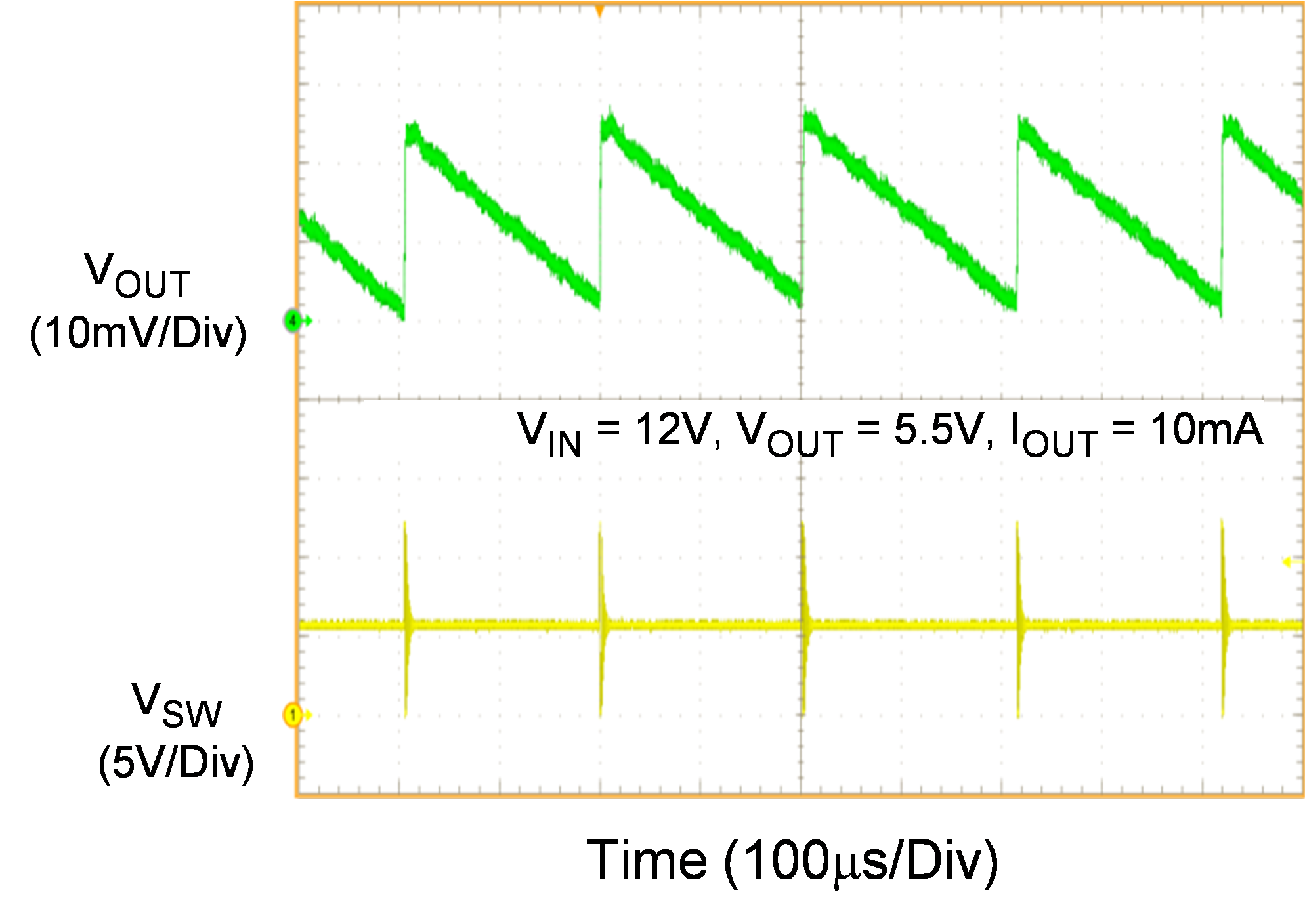
Output ripple at 10mA load: 32mVpp
|
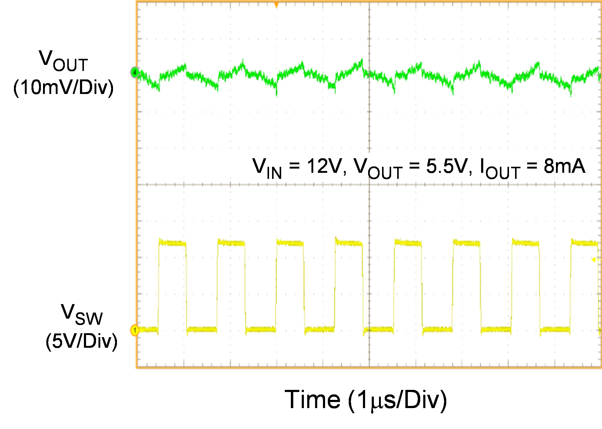
Output ripple at 8A load: 10mVpp
|
|
Output Ripple Measurement
|
Output Ripple Measurement
|
|
|
|
|
Output ripple at 10mA load: 27mVpp
|
Output ripple at 8A load: 10mVpp
|
|
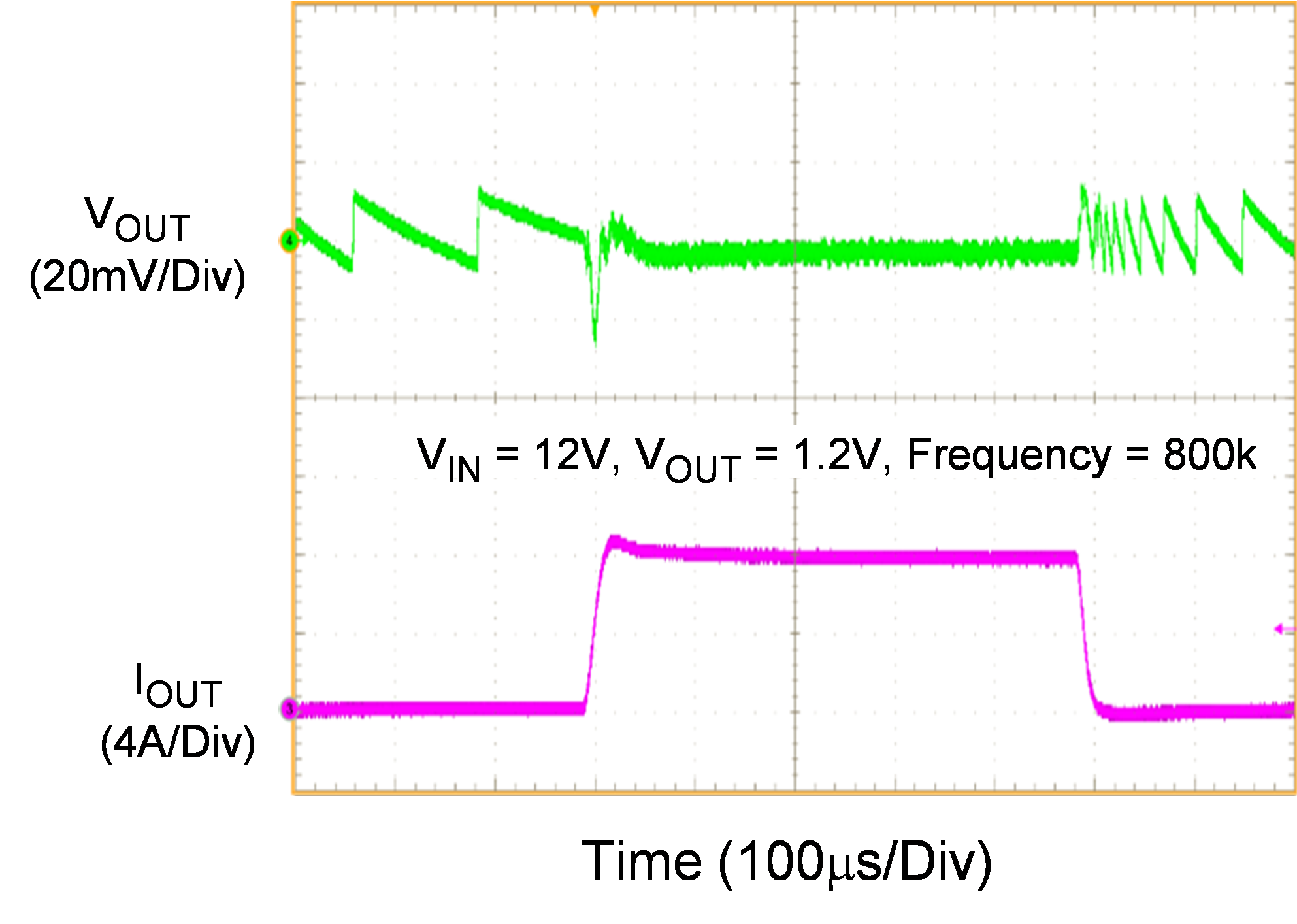
Dynamic Load 10mA to 8A Load Step (DCM mode)
|
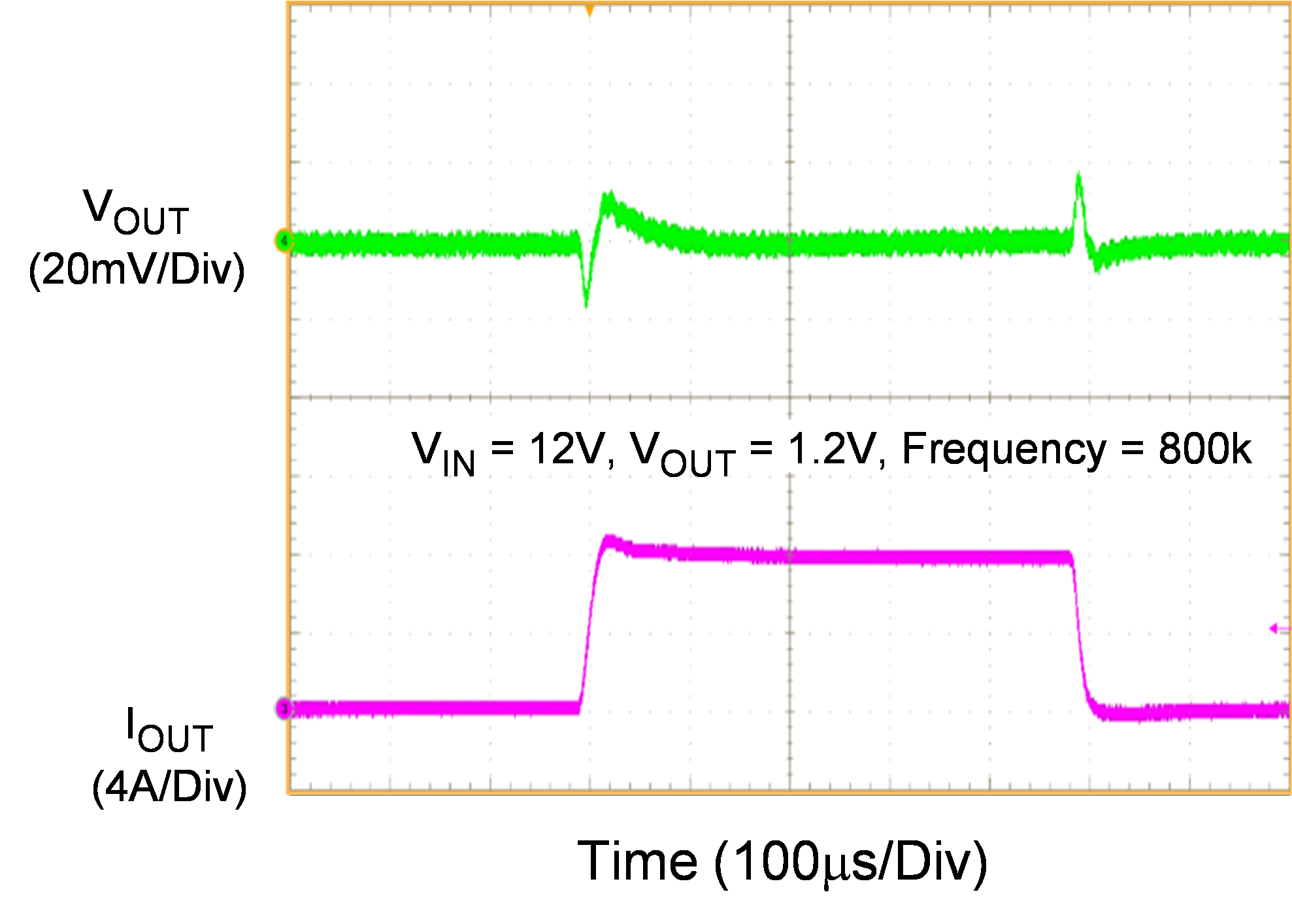
Dynamic Load 10mA to 8A Load Step (FPWM Mode)
|
|
|
|
|
VPK-PK: 40mV
|
VPK-PK: 39mV
|
|
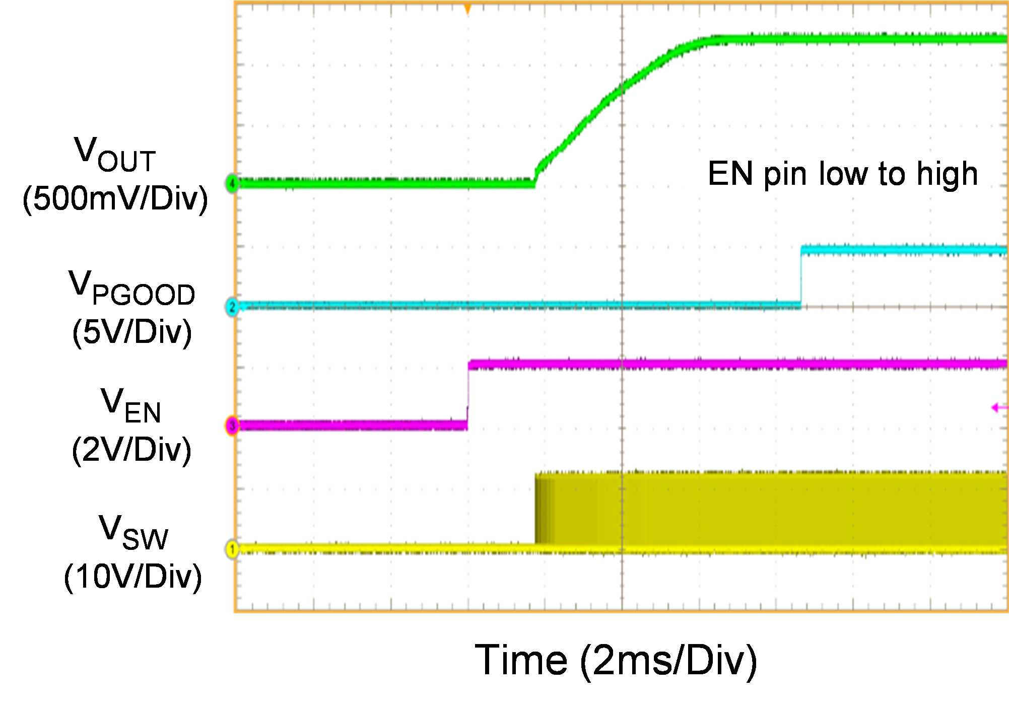
Start-Up Measurement from Enable
|
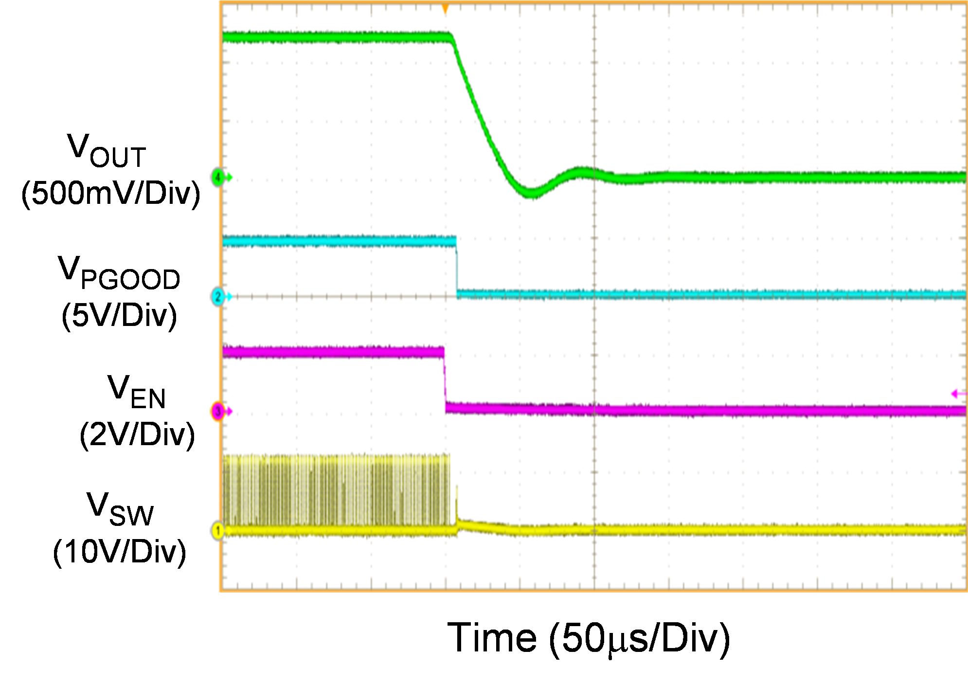
Power-Off Measurement from Enable
|
|
|
|
|
Start-up time 5ms. Soft-start 5ms.
|
Vout discharge during power-off
|
|
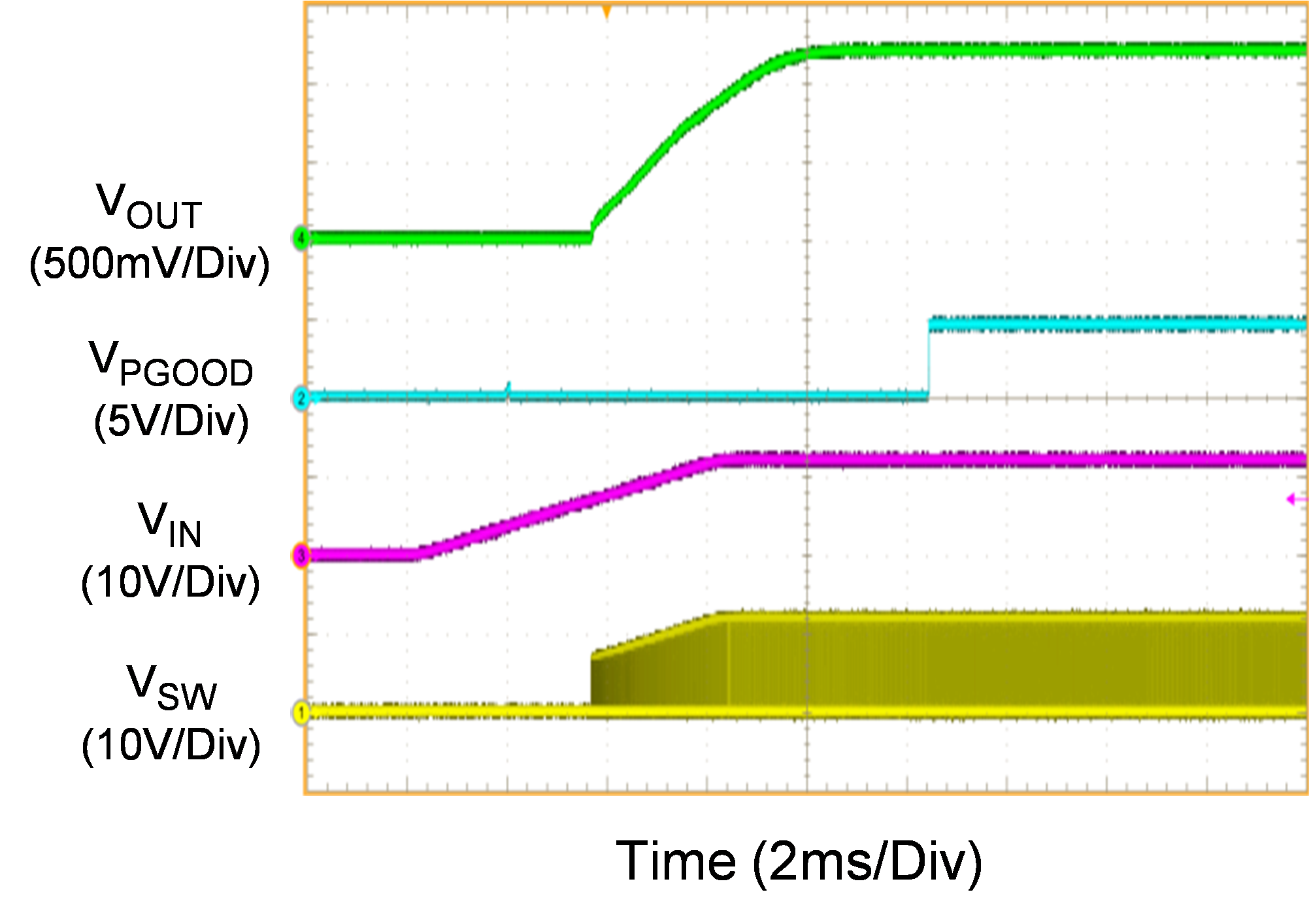
Start-Up Measurement from VIN
|
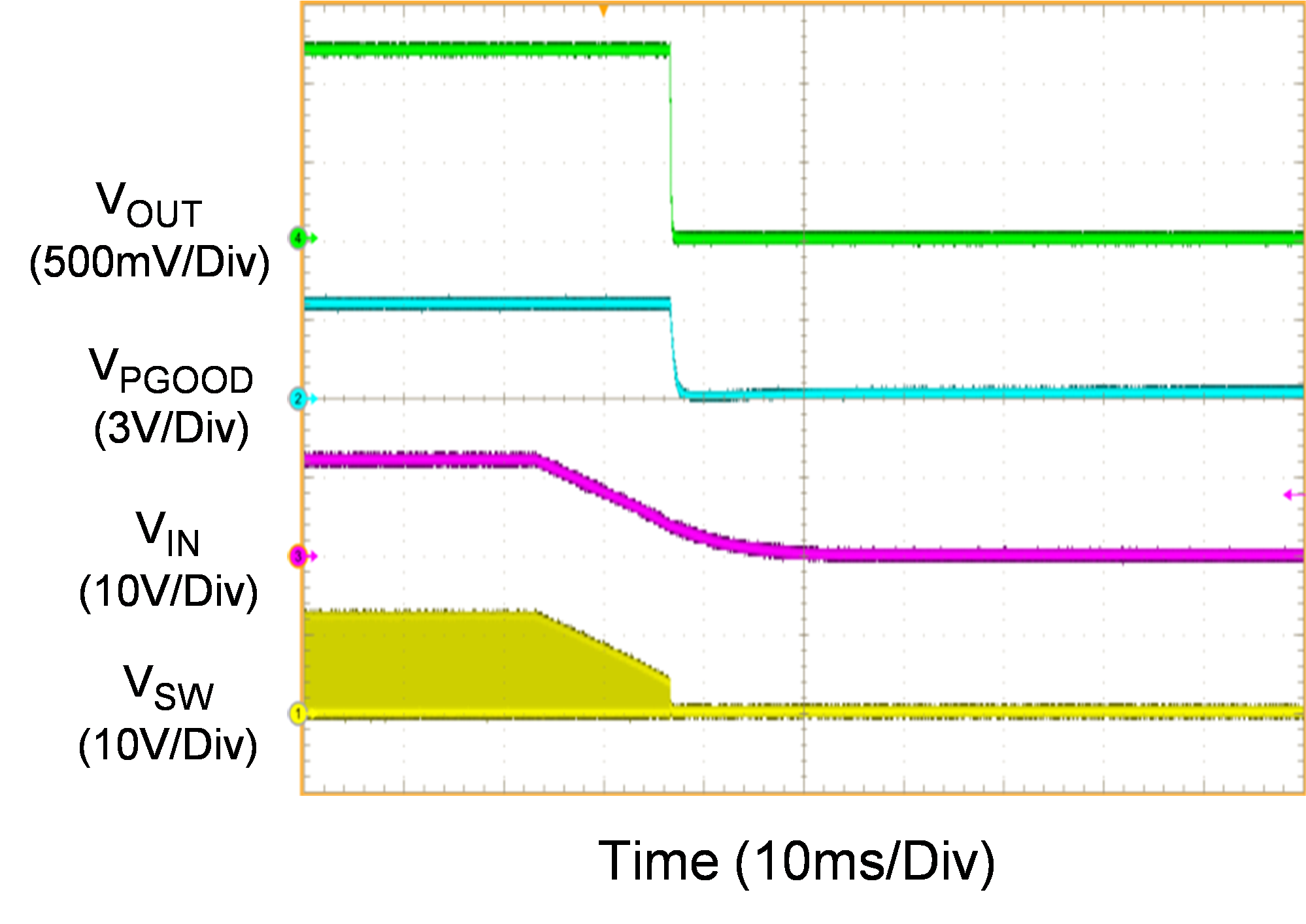
Power-Off Measurement from VIN
|
|
|
|
|
Start-up time 2.7ms. Soft-start 1.575ms.
|
VOUT discharge during power-off
|
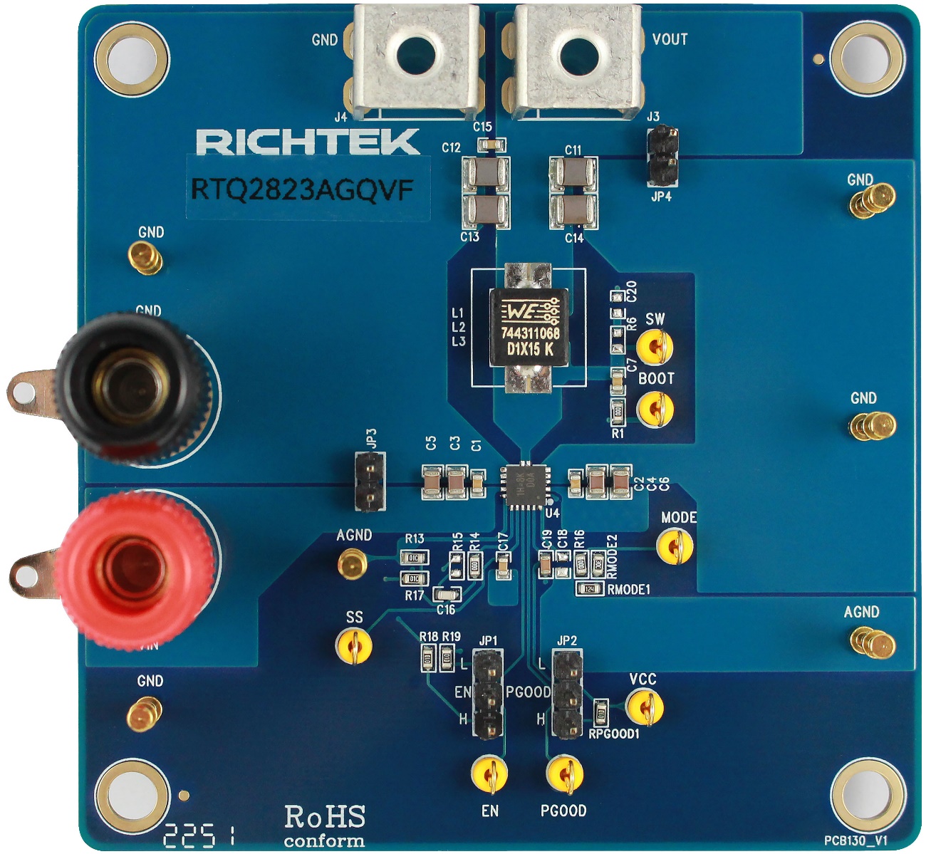
Evaluation Board Layout
Figure 1 to Figure 4 are RTQ2823AGQVF Evaluation Board layout.
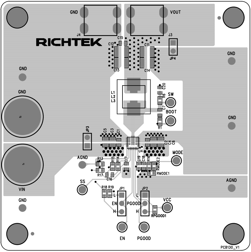
Figure 1. Top View (1st layer)
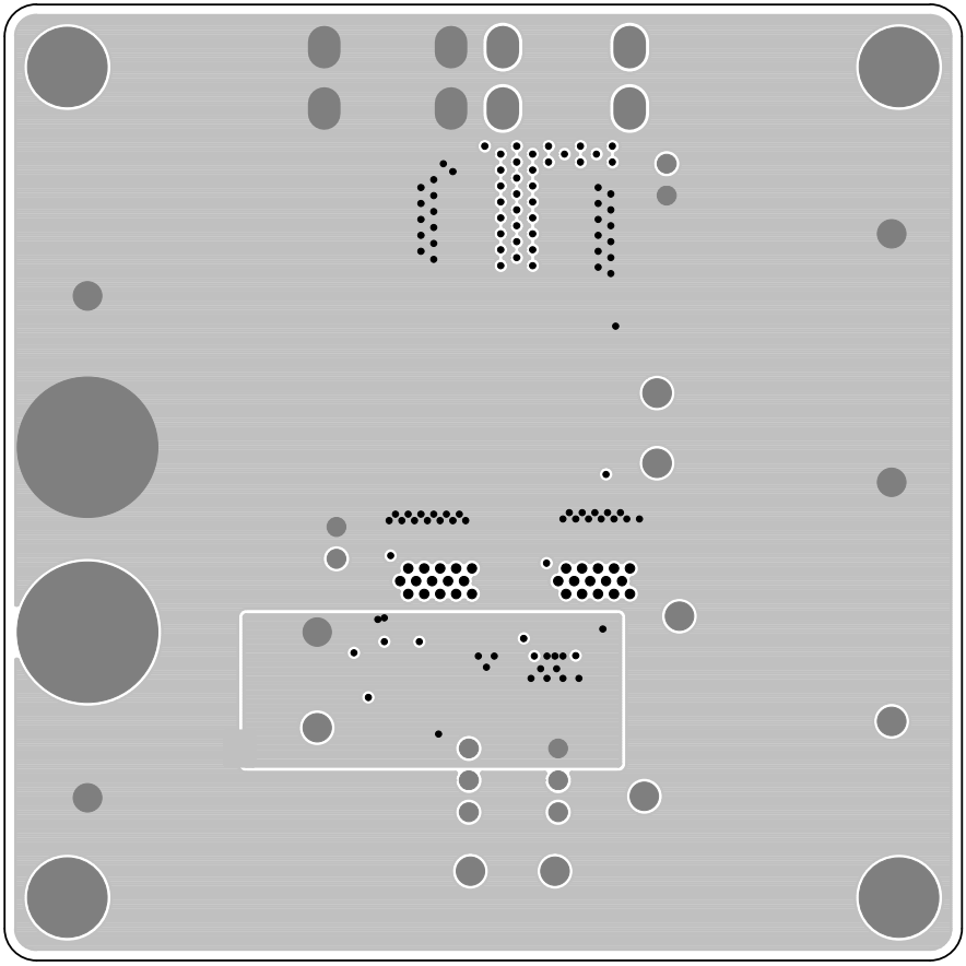
Figure 2. PCB Layout—Inner Side (2nd Layer)
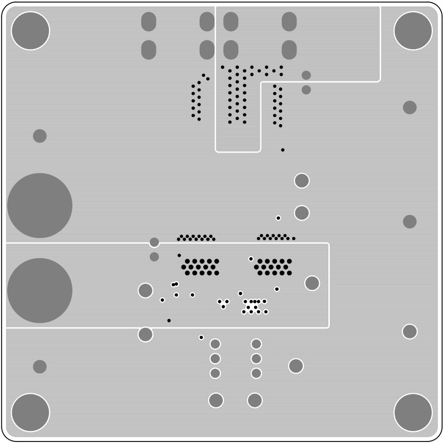
Figure 3. PCB Layout—Inner Side (3rd Layer)
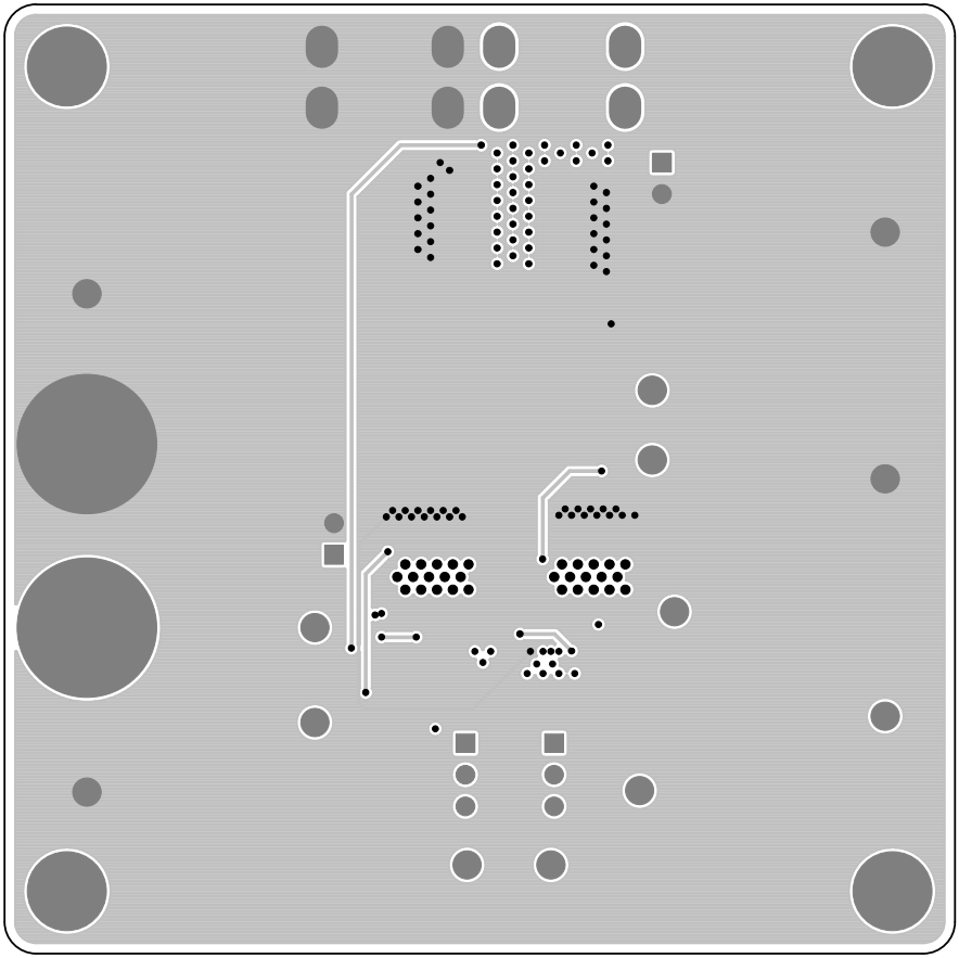
Figure 4. Bottom View (4th Layer)